How a processor is manufactured
 The main component of a certain computer is the processor, and we will see below how it is produced.
 The entire processor is built using the lithography technique, which consists of the emission of ultra-violet lights that are capable of deforming elements such as the silicon wafer through the emission of light.
A processor is not manufactured with even a touch on the surface of the silicon, that is, only the emission of light that causes the components to be generated.
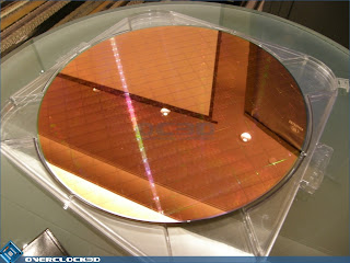
Here is a 30cm silicon plate that is used in the lithography process, which is the process of manufacturing the processors:
Each silicon plate contains several processors next to each other, as this facilitates the manufacture of numerous processors at once, including their transport.
There are 2 most common processor manufacturers today: Intel and AMD. These photos are of processors manufactured by Intel factories.
Note that the processors are glued together. This is the point before the wafer is cut. After cutting, the chip is tested and encapsulated. As per the tests, each processor has different levels of performance, including speeds, so Intel names these processors under other names.
Note the size of the silicon wafer:
Inside the factory, employees are always protected so that breathing does not damage the wafers.
This is because any dust can completely damage some chip in the wafer, as shown below:
The lithography process seems complicated at first, but it consists of the following scheme:
1. The light emitted in a given radiation is emitted.
2. A mask is used to form the desired area, allowing certain areas to allow light to pass through, others not.
3. A lens is used to condense the mask information.
4. A tiny particle of light with the condensed mask arrives on the silicon wafer, thus forming the tracks and transistors.
Notice the image:
After all this process, the processors are cut and tested, and if there is a defect in silicon in any internal component (since there are several internal components, failures can occur in the lithography or in some other process) then this processor has a certain area deactivated and is marketed as a low-cost version, that is, only if the processor does not work in fact it is discarded.
This is the internal part of the processor internally called Dunnington, with 6 cores, using 45 nm lithography technology, 1.9 billion transistors and 16 Mb of L3 Cache.
After that, obviously, the processors are encapsulated and marketed so that they can be used on the motherboards, giving life to the computer.
Image source:
http://www.overclock3d.net/gfx/articles/2008/09/23222540763l.jpg
http://www.legitreviews.com/news/5103/
http://media.forumpcs.com.br/wp-content/blogs.dir/38/files/amd-mostra-wafer-com-processadores-quadrinucleares-de-45-nm/45nm_01.jpg/1200_0,0,0,0/45nm_01.jpg/45nm_01.jpg
http://forum.outerspace.com.br/showthread.php?p=2911834&langid=1
http://www.tecmundo.com.br/intel/2451-processadores-de-32-nucleos-como-isso-e-possivel-.htm
http://www.informetop.com/conheca-os-processadores-intel-i5/
http://www.kerodicas.com/noticias/hardware-2/artigo=23065/


.jpg)
.jpg)


No comments